


How can the tens of billions of transistors in the chip be "installed"?
Transistors are not installed. Chip manufacturing is actually divided into sand wafer and wafer chip. Before chip manufacturing, IC design should be responsible for designing the chip and then handing it to the wafer foundry.
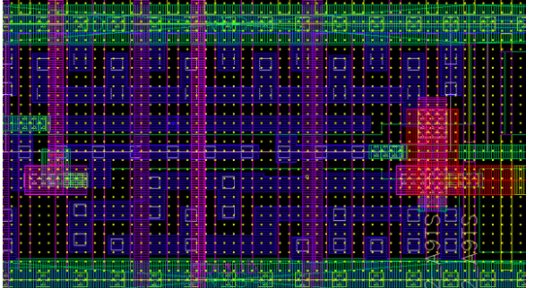
Chip design is divided into front-end design and back-end design. There is no unified and strict boundary between front-end design (also known as logic design) and back-end design (also known as physical design). The design related to process is back-end design. Professional EDA tools should be used for chip design.
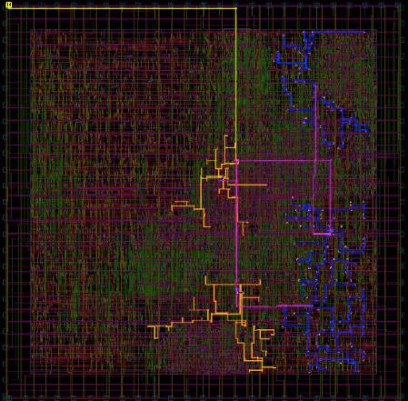
If we amplify the designed gate circuit, the white point is the substrate, and some green frames are the doped layer.
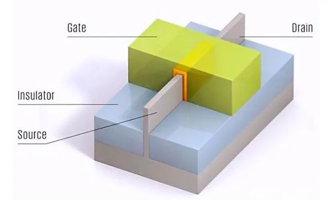
When the chip is designed, it should be manufactured. The transistor is carved directly on the wafer. The larger the wafer, the smaller the chip process, more chips can be cut, and the efficiency will be higher. For example, it's like cutting watermelon. Watermelon is bigger, but it was originally cut into small pieces of 3cm. Now it's changed into 2cm. Is there more pieces. So today's wafers are from 2 inches, 4 inches, 6 inches and 8 inches to 16 inches. The concept of manufacturing process is actually the size of the gate, which can also become the gate length. The shorter its distance, the more transistors can be put down, so that the chip will not become larger due to technological improvement. The more advanced manufacturing process is used, the smaller the area and power consumption of the chip. However, if we change the gate to a small value, the current flowing between the source and drain will be faster and the process will be more difficult.
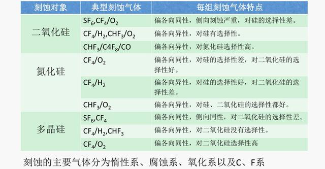
Chip manufacturing is divided into seven production areas, namely diffusion, lithography, etching, ion implantation, film growth, polishing and metallization.
Among them, the two most important steps to carve a wafer are lithography and etching. Lithography is a precision micromachining technology.
Conventional lithography technology uses ultraviolet light with wavelength of 2000 ~ 4500 as the image information carrier, photoresist as the intermediate (image recording) medium to realize the transformation, transfer and processing of graphics, and finally transfer the image information to the wafer (mainly silicon wafer) or dielectric layer.

Lithography is to make the circuits and functional areas needed for chip fabrication. In short, the circuits and functional areas designed by chip designers are "printed" into the wafer, similar to camera photography. The photos taken by the camera are printed on the negative, while the photo is not engraved, but the circuit diagram and other electronic components.
Etching technology is to use chemical or physical methods to remove the unmasked wafer surface or dielectric layer of the resist thin layer, so as to obtain a pattern completely consistent with the pattern of the resist thin layer on the wafer surface or dielectric layer.
The functional layers of integrated circuits are three-dimensional overlapped, so the lithography process is always repeated many times. For example, a large-scale integrated circuit needs about 10 lithographies to complete all the transfer of graphics in each layer.
There are two basic etching processes in semiconductor manufacturing: dry etching and wet etching. At present, the mainstream is still dry etching process, which is called plasma etching machine.
Various types of dry etching processes are required in the manufacturing process of integrated circuits, and their applications involve various materials on silicon wafers. The etched materials mainly include medium, silicon and metal. Through multiple cooperation with lithography, deposition and other processes, a complete bottom circuit, gate, insulating layer and metal path can be formed.
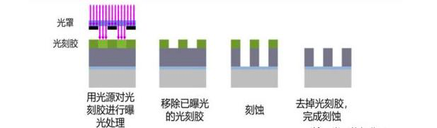
The wafer (or silicon wafer) coated with photoresist is covered with a pre prepared photoresist plate, and then the wafer is irradiated with ultraviolet light for a certain time across the photoresist plate. The principle is to use ultraviolet light to deteriorate some photoresists, which is easy to corrode.
Dissolving photoresist: the photoresist exposed to ultraviolet light is dissolved during lithography, and the pattern left after removal is consistent with that on the mask.
"Etching" means that after photolithography, the deteriorated photoresist is etched off with etching solution (positive glue), and the semiconductor device and its connection pattern appear on the wafer surface. Then another etching solution is used to etch the wafer to form a semiconductor device and its circuit.
Clear photoresist: after the etching is completed, the mission of photoresist is declared to be completed. After all are cleared, the designed circuit pattern can be seen.
Here, what is photoresist. We should know that the circuit design diagram is first written on the photomask by laser, and then the light source irradiates the surface of the silicon wafer with photoresist through the mask, causing the photoresist in the exposed area to have a chemical effect, and then the exposed area or unexposed area is dissolved and removed by development technology, so that the circuit diagram on the mask is transferred to the photoresist, Finally, the pattern is transferred to the silicon wafer by etching technology.
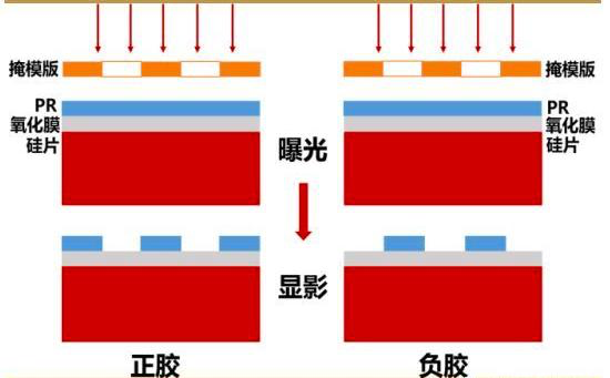
Lithography can be divided into two basic processes: positive lithography and negative lithography. In positive lithography, the exposed part of the photoresist is destroyed and washed away by solvent, so that the pattern on the photoresist is the same as that on the mask.
On the contrary, in negative lithography, the exposed part of the negative photoresist will become insoluble due to hardening, and the mask part will be washed away by solvent, so that the pattern on the photoresist is opposite to that on the mask.
It can be said that in wafer manufacturing, circular silicon wafers with a diameter of 30 cm shuttle between various extremely precise processing equipment, and they make grooves or circuits with a diameter of only one thousandth of the hair wire on the surface of the silicon wafer.
Heat treatment, photolithography, etching, cleaning and deposition... Each wafer has to be continuously processed day and night for two months. After hundreds of processes, it finally integrates a large number of micro electronic devices. After cutting and packaging, it has become the cornerstone of the information society - chip.
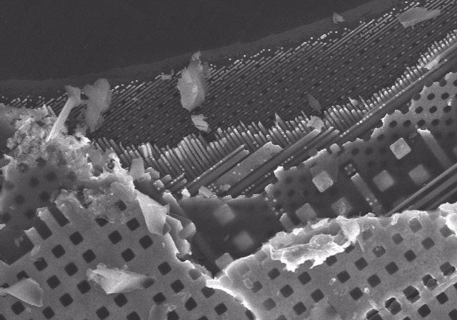
This is a SEM photo of the top-down view. You can clearly see the layered structure inside the CPU. The lower the line width, the narrower and closer to the device layer.
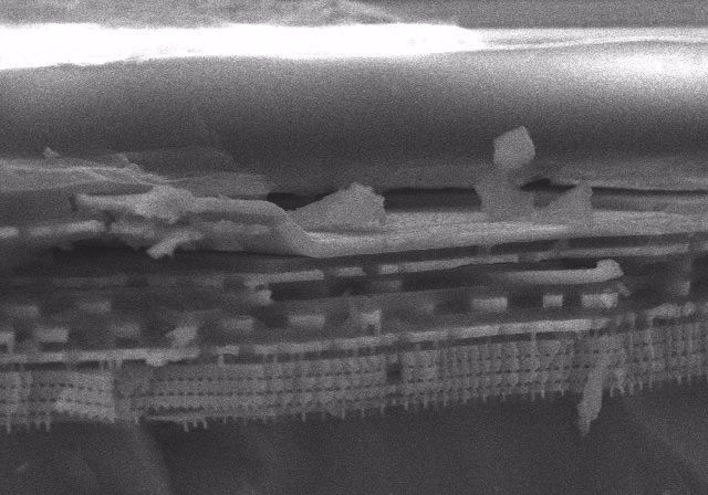
This is the cross-sectional view of the CPU. You can clearly see the layered CPU structure. There are about 10 layers from top to bottom, of which the lowest layer is the device layer, that is, MOSFET transistor.

 Follow us
 +86-755-23763510
 Online service
 mark.xu@gatech-elec.com